Where’s the bias, then?
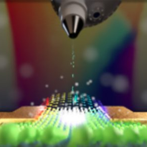
Two-dimensional materials open up new possibilities in optoelectronics, notably through their ability to be freely assembled into heterostructures with diverse properties. This work highlights the importance of finely characterizing the electronic structure of such devices under real operating conditions, revealing - via X-ray imaging - a sometimes unexpected potential distribution in a WS₂/MoSe₂ heterostructure.
References :
Electric Field Distribution within a Van der Waals Heterostructure, Dario Mastrippolito, Mariarosa Cavallo, Erwan Bossavit, Clement Gureghian, Albin Colle, Tommaso Gemo, Giorgia Strobbia, Dries De Pesseroey, Marco Paye, Adrien Khalili, Huichen Zhang, Johan Biscaras, James K. Utterback, Pavel Dudin, José Avila, Emmanuel Lhuillier, Debora Pierucci, Nano Letters 25, 29, 11340–11346. Published: July 14, 2025.
DOI : 10.1021/acs.nanolett.5c02475
Open access : HAL

