
Grain boundaries transform silicon into a plasmonic material
Researchers have shown that films of heavily doped polycrystalline silicon consisting of nanometre-scale grains exhibit plasmonic behaviour distinct from that of conventional metallic layers, raising the prospect of fabricating layers that offer enhanced light-matter interaction without the need for a nanostructuring step.
References:
Mohamad Bahsoun, Jesse Groenen, Gonzague Agez, Sébastien Joulié, Cécile Marcelot, Robin Cours, Sébastien Kerdiles, Mathieu Opprecht, Caroline Bonafos, Jean-Marie Poumirol; Emergence of Localized Surface Plasmons in Unpatterned Hyperdoped Polycrystalline Silicon. Nano Letters 26 (32): 10690–10697 - Published 19 August 2026.
DOI: https://doi.org/10.1021/acs.nanolett.6c01938
Open access: arXiv
Plasmonics, by utilising the collective oscillations of free electrons (plasmon resonances) in metallic or doped semiconductor nanostructures, enables the manipulation of light at the nanometre scale. Major advances in nanofabrication, which have enabled the development of metasurfaces, have contributed significantly to progress in this field. However, despite rapid progress, the large-scale deployment of plasmonic metasurfaces remains limited by bottlenecks related to their industrial manufacture and their integration into functional devices.
This research was carried out in the following CNRS laboratory:
Centre d'élaboration de matériaux et d'études structurales (CEMES, CNRS)
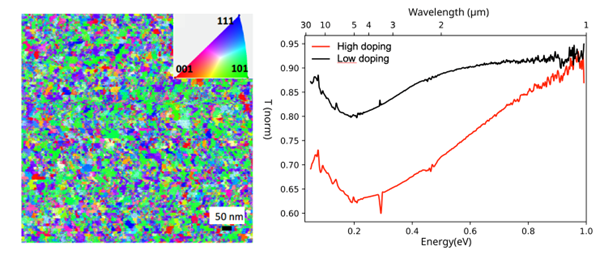
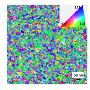
In a recently published study, researchers demonstrate that an alternative approach is possible: plasmonic resonances in the mid-infrared can arise spontaneously in layers of phosphorus-hyperdoped polycrystalline silicon that lack any artificial nanostructuring. Comprising nanometre-sized grains ranging from 5 to 50 nanometres, these layers exhibit remarkable optical properties that challenge conventional strategies for designing plasmonic materials.
By combining advanced techniques in electron microscopy, infrared spectroscopy and electrodynamic modelling, the researchers have shown that these plasmonic responses result from the natural formation of metal–insulator contrasts at grain boundaries. The spontaneous formation of these interfaces between metallic nanograins and dielectric grain boundaries endows the material with plasmonic properties, leading to the emergence of localised surface plasmons.
These results thus position nano-polysilicon as a promising system for the development of sustainable, low-cost plasmonic materials in the infrared spectrum, whilst avoiding the complex nanofabrication steps usually required. This discovery opens up prospects for new applications, such as the manufacture of infrared hyper-absorbers to improve the radiative cooling of photovoltaic devices. This research has been published in the journal ACS Nano Letters.