
3D molecular passivation mapped at the nanometre scale in perovskite solar cells
A team of scientists has shown that the molecular layers used to protect and optimise halogenated perovskite solar cells do not merely act on the surface, but penetrate the upper part of the perovskite film and effectively passivate defects that were previously inaccessible.
References
Dongjiu Zhang, Smail Mostefaoui, Daming Zheng, José Alvarez, Rebeca Lopez-Adams, Jiazhuo Nie, Sergio Vlaic, Yusheng Wang, Baoquan Sun, Philippe Lang, Thierry Pauporté, Lionel Aigouy, Jérôme Aléon, Zhuoying Chen; Beyond the Surface: Three-Dimensional Distribution and Defect Passivation of Self-Assembled Monolayers in Perovskite Solar Cells. ACS Nano, 14 April 2026; 20 (14): 11294–11305.
DOI : https://doi.org/10.1021/acsnano.6c00728
Open Archive HAL
Self-assembled molecular monolayers are commonly used to modify the interfaces of perovskite solar cells and improve charge extraction. Until now, they were generally regarded as two-dimensional surface modifiers.
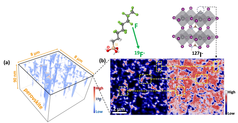
Using high-resolution three-dimensional NanoSIMS imaging, a french team was able to directly track fluorinated molecules deposited on perovskite films. The results reveal that these molecules do not remain confined to the surface, but penetrate nearly 100 nanometres into the film, where they accumulate preferentially in iodine-deficient regions associated with grain boundaries.
This research was carried out in the following CNRS laboratories:
Laboratoire de physique et d'étude des matériaux (LPEM, CNRS / ESPCI Paris - PSL / Sorbonne Université)
Institut de minéralogie, de physique des matériaux et de cosmochimie (IMPMC, CNRS / Museum National d'Histoire Naturelle / Sorbonne Université)
Institut de recherche de Chimie Paris (IRCP, CNRS / Chimie ParisTech - PSL)
Génie électrique et électronique de Paris (GeePs, CNRS / CentraleSupélec / Sorbonne Université / Université Paris-Saclay)
Interfaces, traitements, organisation et dynamique des systèmes (ITODYS, CNRS / Université Paris Cité)
This three-dimensional distribution, previously unseen, changes our understanding of how these molecular treatments work. The fluorinated molecules have several simultaneous effects: not only do they make the surface more hydrophobic, but they also reduce non-radiative recombination, improve resistance to moisture, and passivate defects located at grain boundaries or near the surface. Once optimised, this treatment enables a maximum efficiency of 22.3% to be achieved, representing a relative gain of approximately 8% compared with untreated cells, alongside improvements in current, voltage and form factor. It also enhances the stability of unencapsulated devices, both during storage in humid air and during operation under continuous illumination.
These results demonstrate that certain molecular layers can act as volume-based chemical modifiers, rather than merely as surface coatings. They open up new avenues for designing molecular treatments that target both interfaces and buried defects in perovskite photovoltaic devices. This work has been published in the journal ACS Nano.